This is a progress report on my new Pando keyboard - a split keyboard that keeps the same key layout as the Pando58, but with a completely redesigned PCB and electronics.
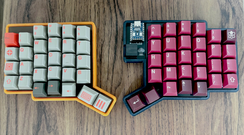
Pando prototype keyboard on the left and the previous Pando58 on the right.
Part of the development of this project was sponsored by PCBWay, who provided a batch of prototype PCBs and a stencil. Their support helped make this build possible.
Ordering through PCBWay was straightforward. The online DFM check caught no issues with my design, and pricing was clear upfront.
The PCB quality was good — boards arrived well-packaged, with clean traces and well-aligned solder mask. The stencil quality was excellent too, though I ended up not using it since the boards it was made for were an early revision that I later revised with more components.
Turnaround was excellent. The PCBs were completed in under 48 hours and the stencil in under 3 days, with detailed production tracking available throughout the process.
Why a new design?
The Pando58 was designed as an easy-to-build kit-first, reliable design.
The new Pando takes it further by exploring an integrated MCU on the PCB. The goal is a no-assembly-required split keyboard while keeping the same philosophy of reliability.
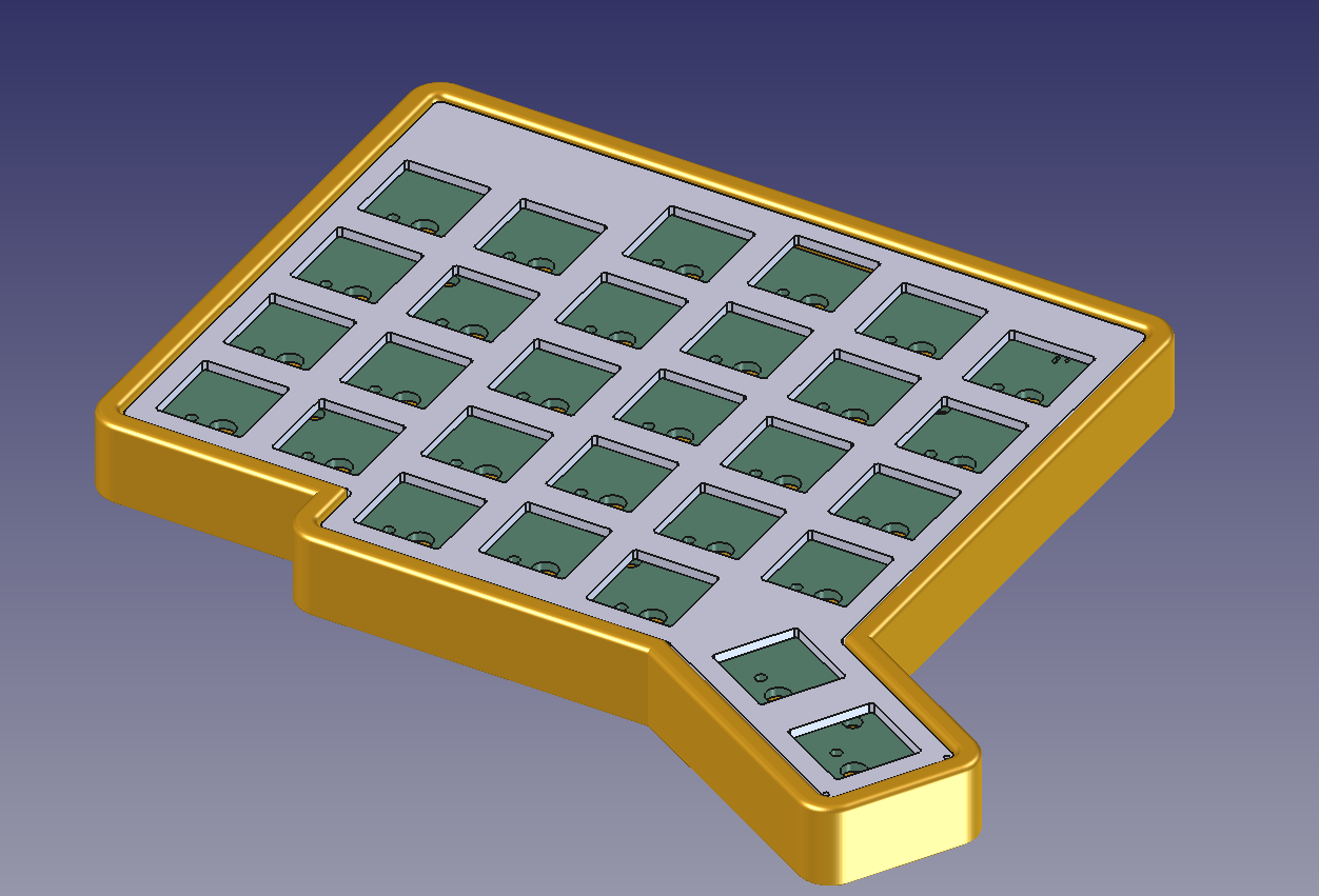
FreeCAD render of the Pando left half case.
Hardware Highlights
Integrated STM32F072CBT6 MCU
No more RP2040 Zero add-on boards. The STM32F072CBT6 is soldered directly onto the PCB.
USB-C Interconnect
The two halves communicate over USB-C. A single USB-C cable connects the left and right halves, carrying I2C between them. Clean, reversible, and sturdy.
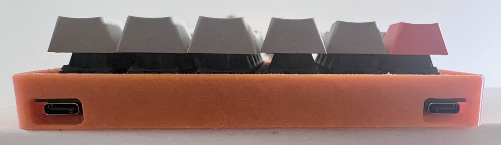
Back side of the left half of the keyboard. Shows USB-C for the PC connection and USB-C for the interconnect. I still need to optimize these USB-C cutouts.
ESD Protection on All Ports
Every external port - the main USB-C to the computer and the interconnect USB-C between halves - has dedicated ESD protection diodes. No more worrying about zapping the MCU during unplugging or handling.
PCA9555 IO Expander (Slave Side)
The right (slave) half uses a PCA9555 IO expander over I2C to read the switch matrix. This eliminates the need for an MCU on the slave side, greatly reducing component count. The interconnect only needs four wires (power, ground, SDA, SCL). Nice and minimal.
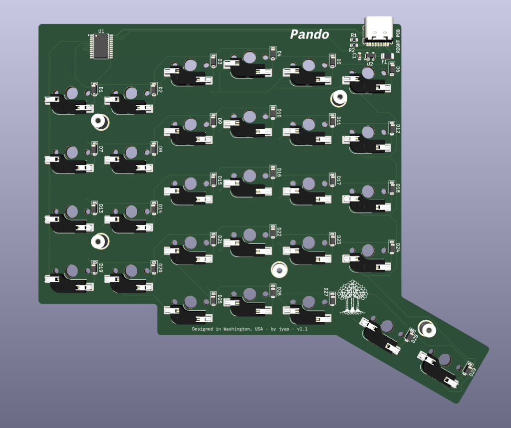
KiCad 3D view of the right PCB with the IO Expander.
Excluding the hot swap sockets, per-switch diodes and mount stand offs, the component count is reduced from 29 components on the master side to just 7 components on the slave side.
0603 Components
All passives are 0603 size. They strike a good balance between ease of placement with tweezers and board space. Small enough to keep the board compact, large enough to not be a headache under the microscope.
Hot Plate + Stencil Soldering
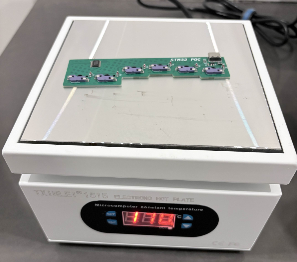
I used a hot plate and stencil to apply solder paste, then placed components by hand and cooked the boards on the hot plate. Part of the proof of concept was proving to myself that a design this dense could be reliably assembled at home with basic tools. And it works.
Firmware
All firmware is working. After some debugging of the I2C communication between the STM32 master and the PCA9555 expander, the matrix scans cleanly on both halves. Keypresses are registered reliably, layers work, and the whole thing is usable as a daily driver configurable with Vial.
The firmware is built with the STM32 HAL and my own matrix scanning / split communication layer.
Keyboard outline - generating the precise physical shape from a layout definition
Footprint placement - positioning all the components. I created an Ergogen configurable Placeholder footprint for this task.
From the Ergogen output, I imported into KiCad for final routing, footprint modification and PCB generation.
Design Process
The project went through several iterations as requirements evolved and lessons were learned along the way.
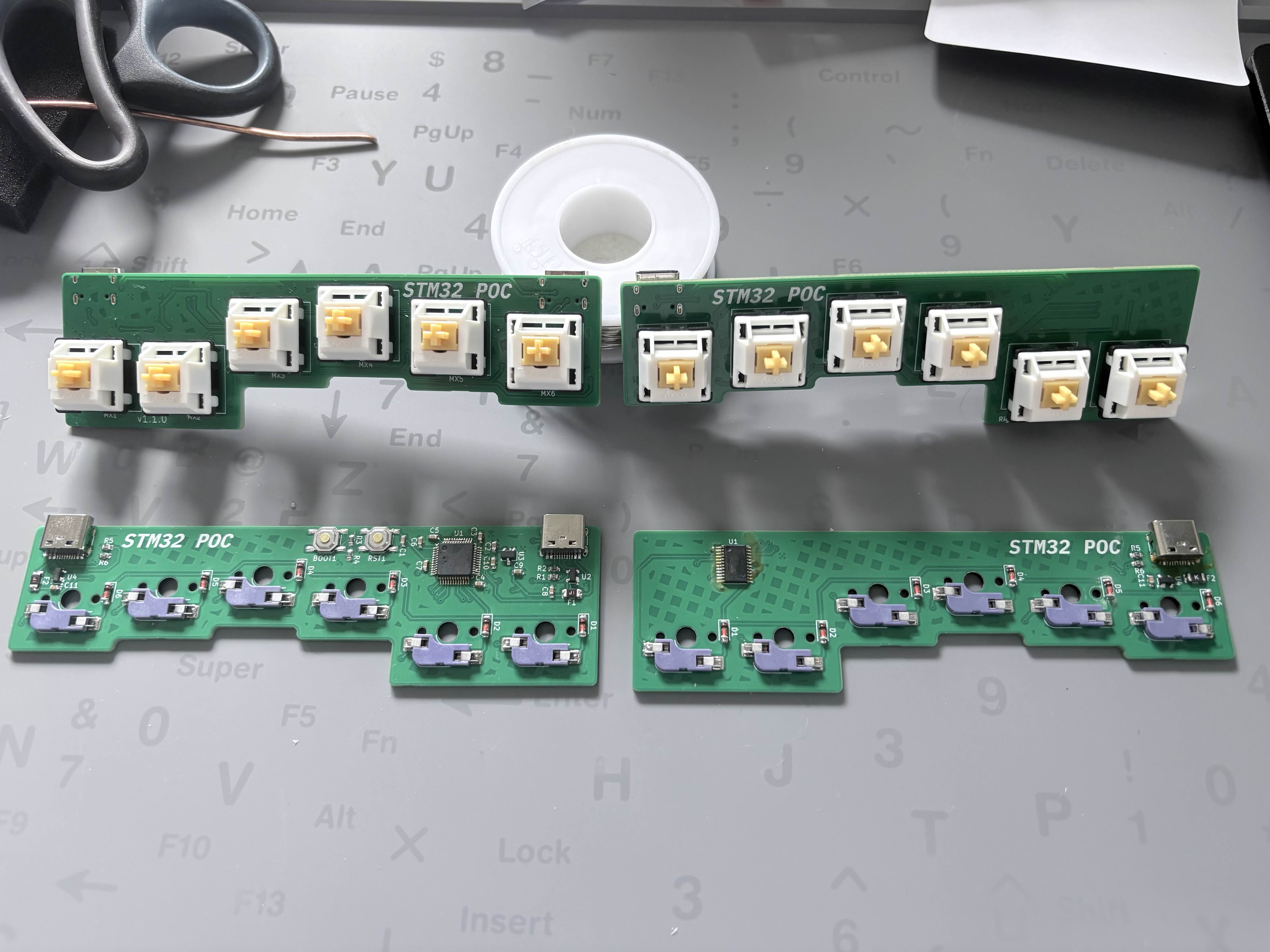
Proof of concept top row of a full split. Top two PCBs are the top side of the left and right halves, bottom two are the respective bottom sides.
Initial Scope
My basic goal was to build an Integrated MCU (prebuilt) split keyboard with the same keycap footprint as my Pando58.
Expansion and Changes in Scope
I set myself a goal of being able to prototype and assemble pre-built PCBs from home.
This meant:
Hand soldering, a hot plate or reflow oven for soldering of components
Hand soldering was impractical and wouldn’t scale.
An oven was more costly, starting at over $280, with little benefit for my use case over a hot plate.
This led to using a hot plate which had me decide on 0603 minimum sized components and designing the PCB with all of the components on the single back side.
Home assembly also meant that while it was more laborious, it was more viable to do small scale production. There is always the option of using PCB Assembly services if production ramps up and the economics justifies it.
Original Assumptions
RP2040
Originally I was planning to use an RP2040 MCU since that seemed appropriate as Pando58 used a RP2040 Zero development board (powered by an RP2040 MCU). RP2040 development boards were considered powerful and capable.
The downsides of the RP2040 MCU are:
It’s more difficult to solder with hidden pads
It requires separate timing crystal and flash storage components
The STM32F072CBT6 solved this. It was easier to solder with visible pins, had an integrated timing crystal and sufficient flash storage.
RJ45 (Ethernet) for Interconnect
Since I had used RJ45 ports for Pando58 keyboard, I thought why not keep it simple and use RJ45 ports but explore different versions like SMT, mid-mount and smaller footprint RJ45 ports.
Early order of parts, many of which were various RJ45 ports which I didn’t end up using.
I ordered a whole bunch of different RJ45 ports but scrapped that once I realized how much extra bulk each port was. It wasn’t really an issue with the Pando58 since the MCU section added extra bulk anyway and the trade off for having hotswap capabilities was worth it.
Since I was going to add a USB-C port anyway, it was a good opportunity to switch to USB-C for interconnect as well. USB-C has a short footprint height and USB-C-to-USB-C cables are abundant and cheap.
MCU on each half
Originally I had envisioned a design with an MCU on each half. This would have been essentially the same design as the Pando58. This changed as I found some split keyboard designs which used IO Expanders. I could see the benefits of using an IO Expander design and no real downsides so added this as a design goal.
PCB Design and Ordering Attempts
It took 3.5 versions of the master PCB to get right (the 0.5 being a bodge of pull-up resistors on the I2C lines). The slave PCB worked first shot - a good reminder of why you prototype with smaller, cheaper boards.
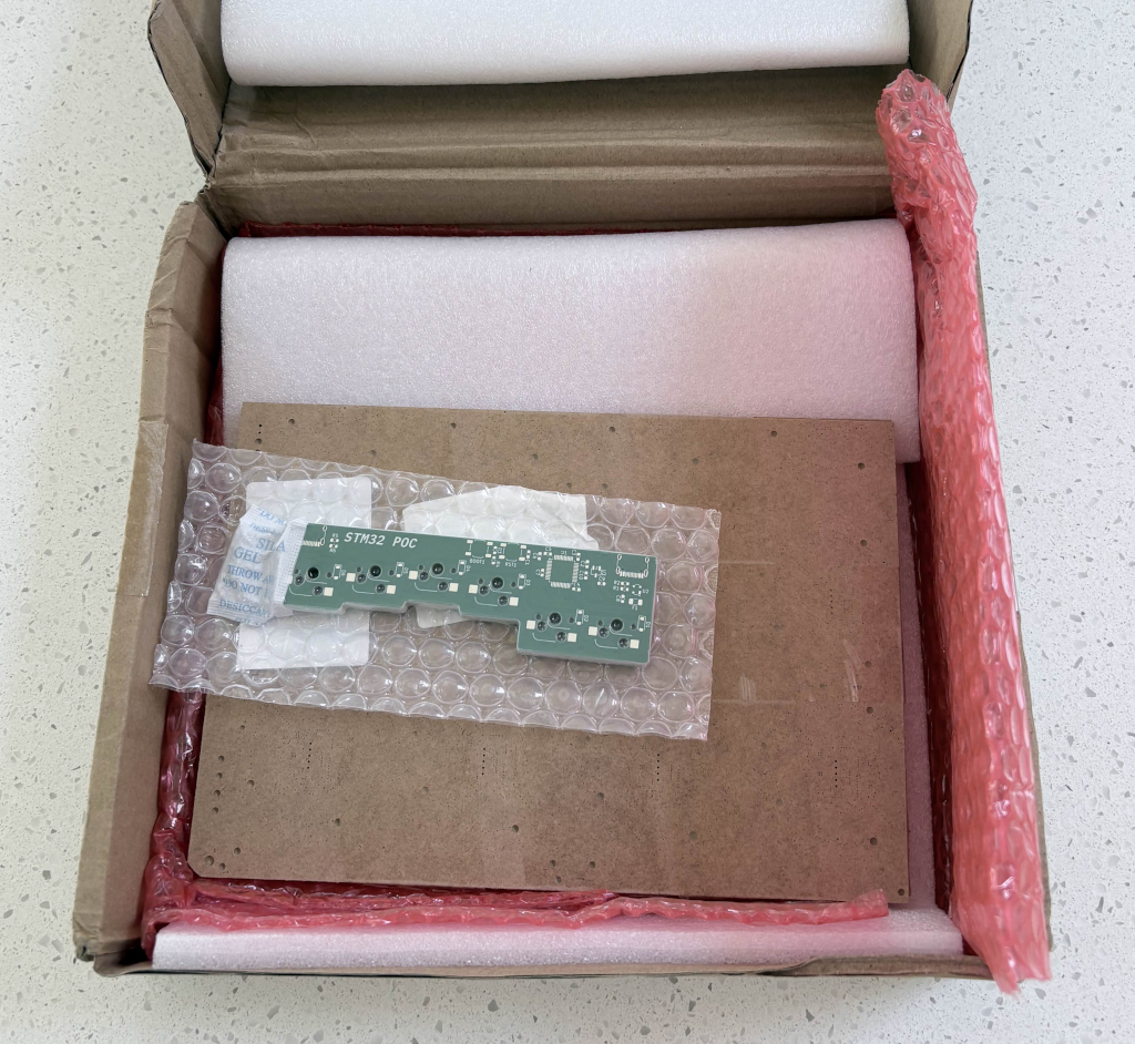
First iteration package from PCBWay - the PCB and stencil in the shipped box.
For the first iteration I ordered through PCBWay, I hadn’t connected the I2C Data lines from the MCU to the USB-C Interconnect port. I also didn’t add ESD protection on the interconnect port.
For the 2nd iteration I connected the I2C Data lines and ESD protection on the interconnect port as well. Unfortunately I did not realize the I2C ports were designated as allocated pin pairs on the STM32.. So I needed to order a 3rd set of PCBs which had these set correctly.
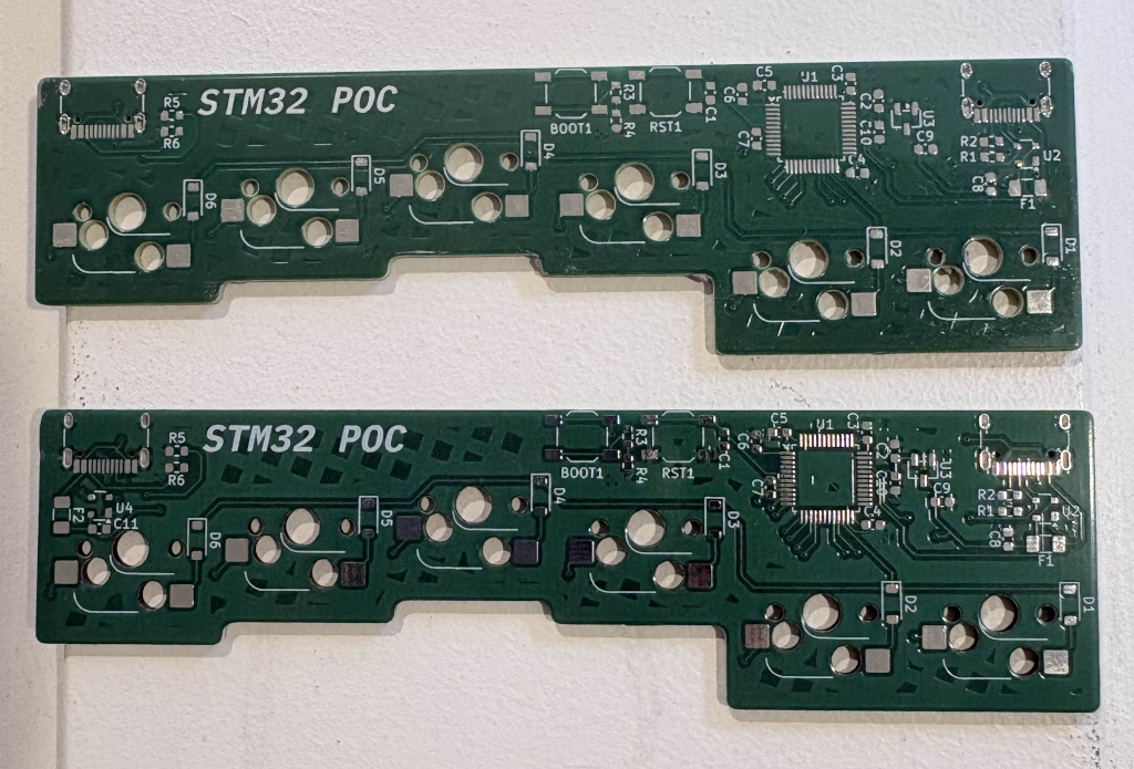
Top PCB is the first version (slightly dirty since I used the unused PCBs as stencil frames), bottom PCB is the 3rd version.
For the 3rd iteration, I correctly added the I2C lines as a pair. Unfortunately I did not realize that I2C lines required pull-up resistors. I bodged on 5k pull-up resistors to each I2C line to the 5V rail.
PCB version 3 with the bodged pull-up resistors on the I2C lines. It’s ugly but it works.
I ordered the first set of master PCBs thinking I would have everything right. I added in the pull-up resistors.. Except I didn’t connect them to the 5V rail.. As of writing this, I will need to order a new set of master PCBs with the correction and hopefully that will work.
On the plus side, the slave PCBs worked first time. The simplified design with the IO Expander was a real benefit here as less components means less things that can go wrong.
Iterative Hardware Testing
Single Side Build
This was the first test I performed. I wrote the firmware and tested a single side.
This worked fine which proved that the overall PCB design with the integrated MCU was correct.
Hot plate in action heating up and soldering components onto a PCB.
This was also my first experience working with the hot plate. I did need to do some drag soldering to fix up some parts but overall this was a big breakthrough and demonstrated that home assembly was viable.
2 MCU Design (3-Wire Interconnect)
This worked fine as well. It demonstrated the USB-C interconnect was designed correctly. It was set up to run over 3-wire split (single pin UART).
This design would also be a fall back if the IO Expander did not work.
1 MCU with IO Expander Slave
This took a while to get working.
Firstly, this set up isn’t a simple JSON configuration in QMK to get running with firmware (unlike the single MCU build and 2 MCU design). When you use an IO Expander you need to write lower level code, specifically your own matrix scanning code.
It took a bit of testing to make sure things were communicating correctly.
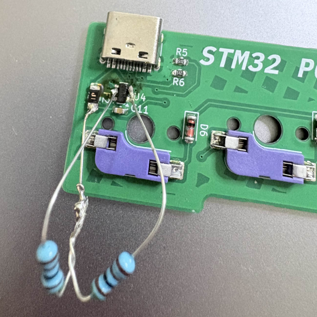
For one thing I didn’t know I2C only drives signals low, relying on external pull-up resistors to pull them back high. I had to bodge some pull-up resistors onto my Proof of Concept MCU. This worked and I further updated my PCB design.
I got this all working with the correct code and settings. This proved to me that the full version would work perfectly.
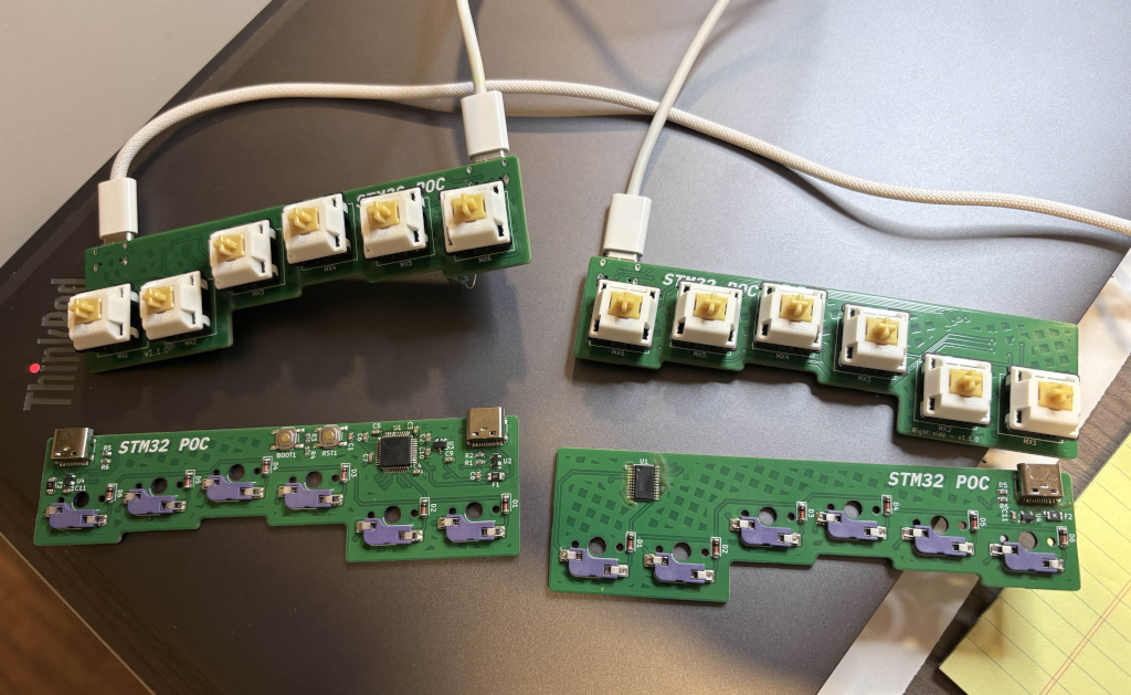
Fully populated working version of the left side with the MCU and the right side with the IO Expander. The top PCBs are the front side and the bottom PCBs are the back sides of the respective PCBs showing the populated components.
I can definitely recommend prototype testing on a small scale to keep the costs down for manufacturing and shipping. In my final versions of the full sized PCBs, it was a matter of adding in the missing rows, thumb cluster and extra row routes.
Materials testing
POM (also known as Delrin or Acetal)
POM is a common switch plate material which is also known by the brand name Delrin or Acetal. I have access to a makerspace CO2 laser cutter so it was a good option to test out sourcing raw materials and cutting.
Pictured below is a cut sheet I bought from Amazon.
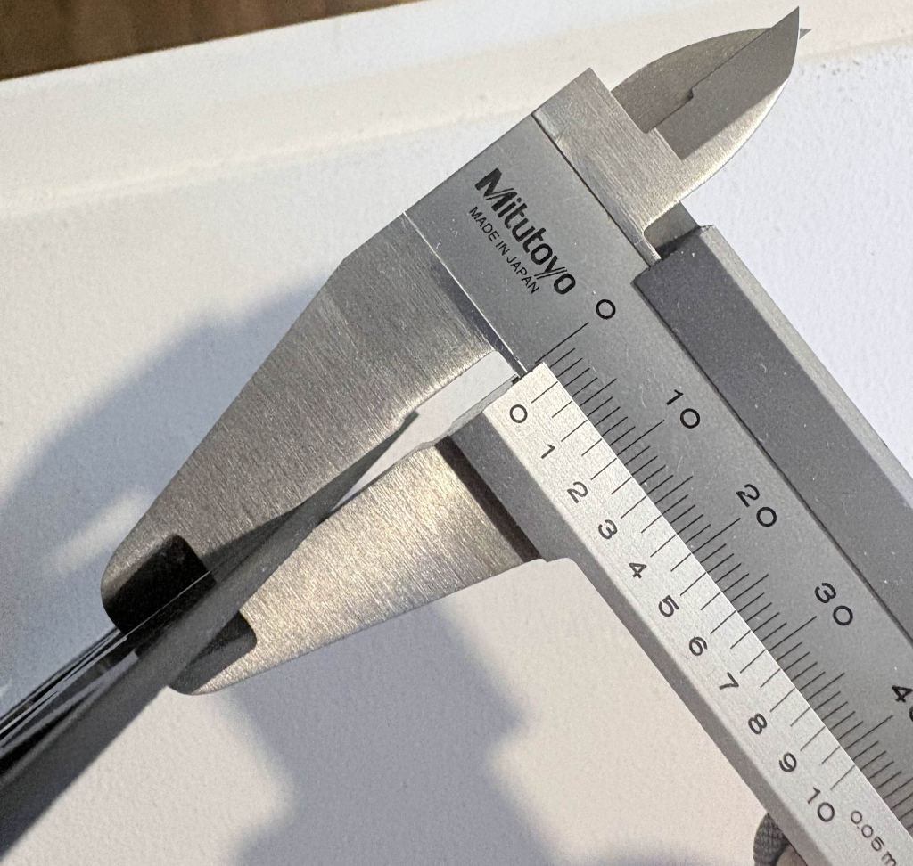
Measurement of a cut Acetal sheet bought from Amazon advertised as 1/16 inch (1.5875 mm) but measuring 2.3 mm - significantly thicker than advertised.
Per the image description, unfortunately this raw sheet was way out of advertised specifications for thickness so switches didn’t snap on properly.
I bought a couple of sheets from McMaster-Carr which have proper tolerances advertised and measure up perfectly.
I cut those up with the CO2 laser but found some issues. The kerf and tolerances were an issue as well as heat from the laser which led to warping. I needed to shrink the switch openings gradually until the switches snapped snugly in place.
I managed to flatten out the POM switch plate using my hot plate and a method of heating it up to 150 degrees Celsius, allowing it to cool and weighing it down overnight. Unfortunately the flexible nature of POM, probably combined with the shrinking of the switches made it a bad fit.
I may revisit this using CNC to cut a POM plate.
MJF - Multi Jet Fusion 3D printing
MJF is a form of 3D printing.
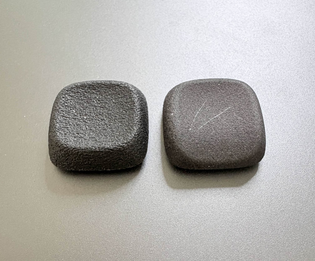
MJF 3D printed sample keycaps. Left is PA12-HP Nylon, right is PA12S-HP Nylon.
I printed out sample keycaps in PA12-HP Nylon and newer PA12S-HP Nylon. PA12S-HP Nylon is a newer offering that comes out smoother but unfortunately scratches easily which is quite the dealbreaker.
PA12-HP Nylon is more textured but does not have the scratch problems.
A MJF case (perhaps with an integrated switch plate) is something I plan on testing.
Things That Went Wrong
Slow flashing
Flashing the firmware to the STM32 MCU using dfu-util was slow and took 5 minutes per flash which greatly increased the time it took me to test and debug. The REPL loop was brutal. It took me a good 2 days to get the IO Expander to work because I would often set the board to flash and walk away.
When it was all said and done, I had time to look up the delays. I found a similar reported issue for dfu-util and built it from source to test it out… To my surprise the STM32 flashed in a few seconds… This would have saved me a lot of time and frustration.
I wrote a patch to my Nix environment which will allow me to reap the benefits of the fast flash times by default.
IO Expander stopped working
At one point the IO Expander just stopped working.
After testing it looked like 5V wasn’t pulled up consistently on the I2C lines. I built a new master PCB with new bodged resistors and it started working again. The conclusion is that bodged resistors can be inconsistent and actually increase the resistance.
I will need to test out the voltage pulled across when I create my next (and hopefully final) master PCBs. In theory it should all be cleaner voltage.
What’s Next
Case design improvements (MJF 3D printed and powder coated metal).
Real life dogfooding and testing of the keyboard. I have been testing it by running with the left half with no issues but I will need to use and daily drive the full build.